I put the antennas below to make the coax routing easier to the wifi card. I’m not sure how possible it would be to have them above the board and then making the bends without exceeding the radius turn limits for most cables.
The NVMe isn’t accessible. Could probably make a snap plate or something for that.
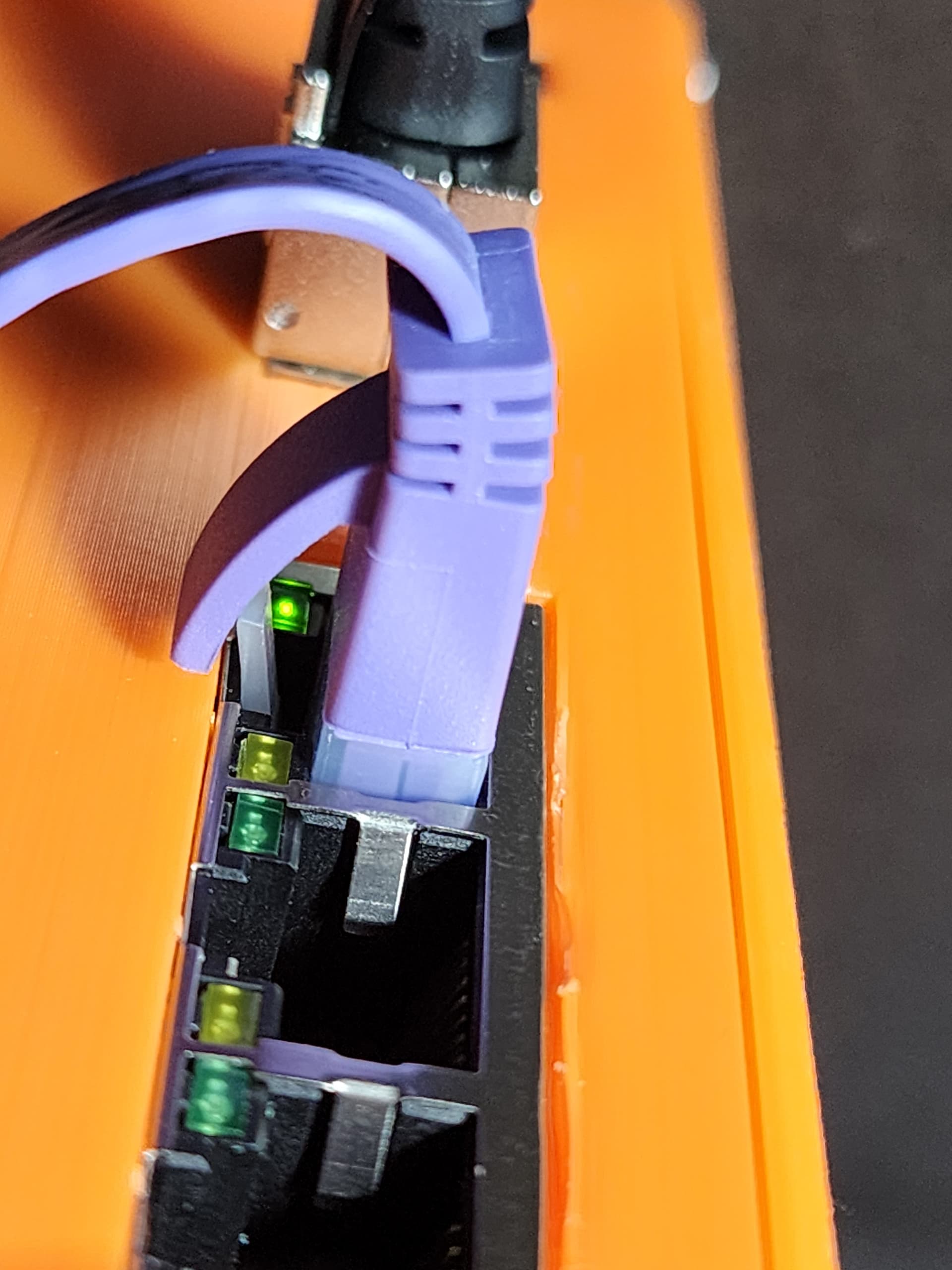
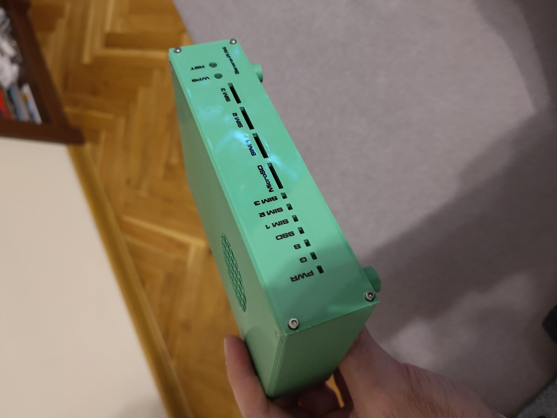
The RJ45’s are actually nearly flush mounted. The clip doesn’t touch the case. The RJ45 block seems to be ~0.25mm offset from the other ports (sfp cages, power), otherwise it would be flush.
Sounds logical…is right/left not enough space for the cables in larger radius? But yes,compared with r3 wifi is on bottom,so it makes sense having antennas also below board.
Ok,then it was a optical illusion in first picture in previous post. Sorry for the noise.
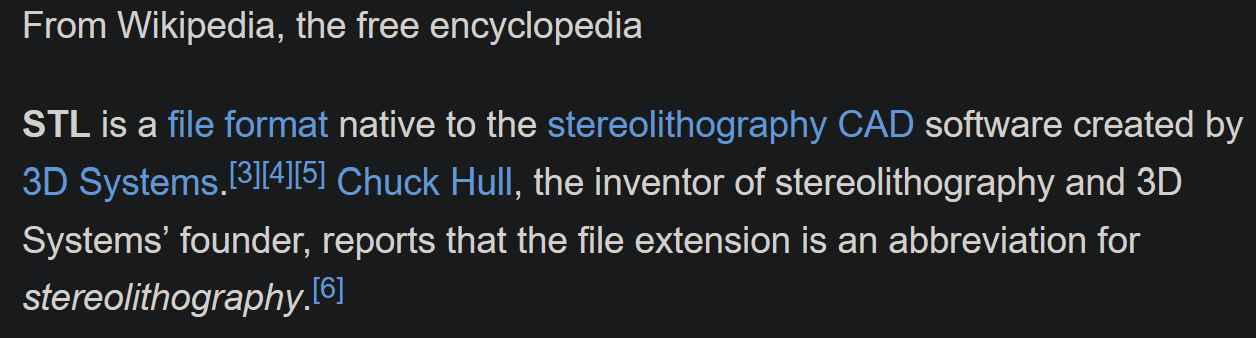
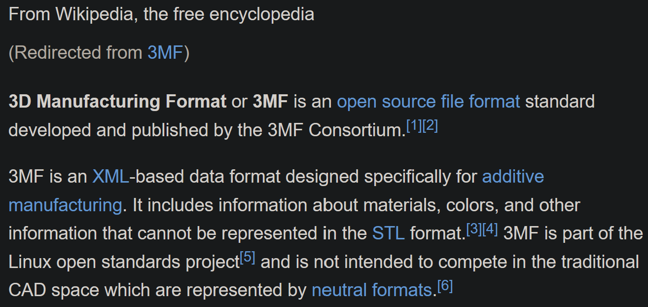
Here’s the STL files. Issue with STL files on something like this, is 3MF each component is still individually unique. So you can include multiple components, see them assembled, but then only print out the objects you need.
About every slicing software should support a 3mf file with preview.
Enough space that you could probably fit several dozen RG174 cables, but I would be more concerned with the bend radius compressing the dielectric core and attenuation. The bulkhead connector I have there is a standard machine produced one, it’s a few cm on the heat-shrink tube.
One possibility would be to go across the top of the board to the opposing side before looping down. This would decrease any bend diameters, but making for some long runs while possibly picking up some weird EMI off the chips and power regulator. (honestly would be interesting on the effects without a RF shield in place)
Ok,then it was a optical illusion in first picture in previous post. Sorry for the noise.
hah, no problem. high contrast material, trying to use my magnifying loop light, and a cell phone for pics, it’s bound to lead to weird pictures.
The font I used is Microgramma D Extended. Don’t forget to enable mirrored output and disable scaling when printing on the transparency.
Also important – your bed must be trammed as usual (you should not take into account the additional thickness of the transparency foil). The additional squish of the molten plastic makes the final finish completely smooth and flat (no lines as with the normal 3d printing first layers), and it makes sure the toner gets transferred.
The RJ45 block and the SFP cages should be mounted flush on the board. There’s probably a small deviation, but I had put in the recommended tolerance of 10.20 and 15.15 on them to allow. On the RJ45 block I had added an extra 0.25mm to the sides and 0.40mm to the height to allow for tolerances. (recommended tolerances are not listed in the specs document)
The USB-C plug with the current case should allow for a 0.1mm to 0.2mm clearance on the minimum USB-C size specifications of 6.51mm minimum of exposed shell/gnd. (https://www.usb.org/sites/default/files/USB%20Type-C%20Spec%20R2.0%20-%20August%202019.pdf page 57) You should be able to slide 1~2 sheets of paper between the non-exposed cable shell and the case.
With 3D printing, there are several other factors that start coming into play. Material shrinks, and the nozzle diameter maters. In the slicing software if you have something that’s 2mm thick, its actual thickness will be determined by the line width. Printing something with 0.4 and 0.8 will lead to slight differences. The slicer software can hide some of these facts, so attention needs to be paid in the settings.
Shrinkage of the material will also play a factor. PLA you can expect ~0.5%, ABS and you can start approaching 2%. While it doesn’t sound like a lot, you print something that’s 150mm and it shrinks 2%, it’s going to be 147mm when it cools.
Actually, looking at the original sized pics that you had posted there, there’s something wrong with the mounting of the board or the print.
The SFP cages should be flush with the face, but in the pic it looks like yours are back 1~1.5mm. (PCB setback is 6.875mm)
The RJ45 block should be almost flush, like ~0.15mm at most away from the face (PCB setback is at ~6.74 mm)
The DC jack will also be the same as the RJ45 block, either flush or just slightly recessed. (if I print using a 0.4 nozzle, it’s flush, a 0.6, it’s slightly recessed)
On the inside, the board should be flush against the inside face.
If you don’t have the SFP cages flush with the front, then you won’t actually be able to insert any modules into them because the case will keep them from being able to insert all the way due to the module locks on the bottom. I’m using DAC and 10Gbit modules in mine and they fully insert correctly, locking into place.
Thanks! I just ordered a bpi-r4, barebones. I have to wait a few weeks for shipping. In the meantime, I’m keen to print a case for it. Just leaving a comment here so you know there’s still interest from the masses.
Really nice.
Would you have the files in a format that would be compatible with easy editing in FreeCad ?
I’ve a 5G modem on the top slot and need 4 holes for the antennas above the PCB.
AsiaRFs’ Paul Lai just responded to my email where he says,
“Kindly be noted the single mini PCIe or M.2 module will be available in next month.” [emphasis added], referring to the Wifi 7 board for the Banana Pi BPI-R4.