Actually, there is more info to dump…
/*
* Description:
* a) Optical transceiver EEPROM read/write transactions are just like
* the at24 eeproms managed by the at24.c i2c driver
* b) The register/memory layout is up to 256 128 byte pages defined by
* a "pages valid" register and switched via a "page select"
* register as explained in below diagram.
* c) 256 bytes are mapped at a time. 'Lower page 00h' is the first 128
* bytes of address space, and always references the same
* location, independent of the page select register.
* All mapped pages are mapped into the upper 128 bytes
* (offset 128-255) of the i2c address.
* d) Devices with one I2C address (eg QSFP, CMIS) use I2C address 0x50
* (A0h in the spec), and map all pages in the upper 128 bytes
* of that address.
 *	e) Devices with two I2C addresses (eg SFP) have 256 bytes of data
 *		at I2C address 0x50, and 256 bytes of data at I2C address
 *		0x51 (A2h in the spec).  Page selection and paged access
 *		only apply to this second I2C address (0x51).
* e) The address space is presented, by the driver, as a linear
* address space. For devices with one I2C client at address
* 0x50 (eg QSFP, CMIS), offset 0-127 are in the lower
* half of address 50/A0h/optoe_client. Offset 128-255 are in
* page 0, 256-383 are page 1, etc. More generally, offset
* 'n' resides in page (n/128)-1. ('page -1' is the lower
* half, offset 0-127).
* f) For devices with two I2C clients at address 0x50 and 0x51 (eg SFP),
* the address space places offset 0-127 in the lower
* half of 50/A0/optoe_client, offset 128-255 in the upper
* half. Offset 256-383 is in the lower half of 51/A2/dummy.
* Offset 384-511 is in page 0, in the upper half of 51/A2/...
* Offset 512-639 is in page 1, in the upper half of 51/A2/...
* Offset 'n' is in page (n/128)-3 (for n > 383)
*
* One I2c addressed (eg QSFP, CMIS) Memory Map
*
* 2-Wire Serial Address: 1010000x
*
* Lower Page 00h (128 bytes)
* =====================
* | |
* | |
* | |
* | |
* | |
* | |
* | |
* | |
* | |
* | |
* |Page Select Byte(127)|
* =====================
* |
* |
* V
* ------------------------------------------------------------
* | | | |
* | | | |
* V V V V
* ------------ -------------- --------------- --------------
* | | | | | | | |
* | Upper | | Upper | | Upper | | Upper |
* | Page 00h | | Page 01h | | Page 02h | | Page 03h |
* | | | (Optional) | | (Optional) | | (Optional |
* | | | | | | | for Cable |
* | | | | | | | Assemblies) |
* | ID | | AST | | User | | |
* | Fields | | Table | | EEPROM Data | | |
* | | | | | | | |
* | | | | | | | |
* | | | | | | | |
* ------------ -------------- --------------- --------------
*
* The SFF 8636 (QSFP) spec only defines the 4 pages described above.
* In anticipation of future applications and devices, this driver
* supports access to the full architected range, 256 pages.
*
* The CMIS (Common Management Interface Specification) defines use of
* considerably more pages (at least to page 0xAF), which this driver
* supports.
*
* NOTE: This version of the driver ONLY SUPPORTS BANK 0 PAGES on CMIS
* devices.
*
**/
I can’t check now, but we can use ethtool -m eth1 page N hex on to examine more on 0x51
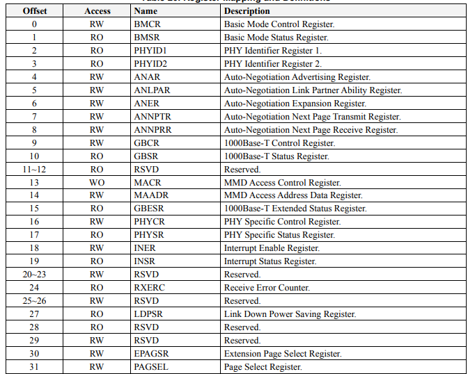
If 0x56 is indeed a rtl8221, then the registers at 0x56 should be (counted in 16 bit words, from rtl8211 datasheet, I cannot find any datasheet of rtl8221)

Since the id is at 2 and at 14 this could actually make sense, as the sfp was trying to access the phy_id (from MMD). Guess this was the last succesfull communication…
The last 4 bytes of the 64 byte space are to do with page selection. This could explain why @frank-w 's module reads totally different. writing 0x0000 to word 31 (byte offset 62) should set the page to page 0.
So maybe @dangowrt has a datasheet of the RTL8221B-VB-CG that he could maybe share or maybe could not. Maybe see if MAADR register is 4 bytes on RTL8221, which would make sense of the data I see?

