carrier aggregation 3x or no?


Is it still possible to replace the soldered-in EMMC with the soclet like on a pic to make it replaceable?
As for me it’s a better option.
Thank You!
Hi, If it still possible, please:
- Add pci lanes to M2. key B interface
- Remove components(capacitors, SIM slots) and check clearenace under the modem (the Telit modem, maybe others) have components on bottom side.
- Create wide clearance around M2. key B socket (look at MeiG and Cinterion 5G modems)
- Route additional USB type C connector from M. 2 interface for modem debug port (QXDM, MTK, UNISOC debug tools)
- If possible, add SMA connectors to edge of board, that can be connected with RF cables from the 5G modem.
And I waiting to order it for use as 5G modems testing in our 5G labs.
Thanks, Dmitry
Can it be powered by the USB-C connector with PD?
Does it use the FUSB302 like some other boards? There is a lot of trouble using this one.
I’m also very interested and want to know when to buy and the price.
Hi,Frank, Thank you for the suggestion, if possible, it will be improved in the next version
The standard board supports one USB3.0 M.2 4G/5G and two USB2.0 miniPCIe 4G modules.
It can also be customized to support two miniPCIe 5G modules of USB3.0. Of course, because the USB3.0 and PCIe interfaces are co-pad, there will be no PCIe3.0 2lane function after the modification.
In addition, minipcie’s wi-fi 7 NIC and 4G are optional.
The reliability of this kind of module is not as good as that directly soldered on the board.
If you want to increase the capacity, maybe you can insert NVME SSD. eMMC is used for storage systems and general applications.
Hi, Dmitry.
Thank you very much for your suggestions.
We have considered these in the first version of the design, but because the board is not big enough, we put the components under the module, and according to the test results, some more components may be added. In addition, it is almost impossible to add USB typeC and SMA connectors.
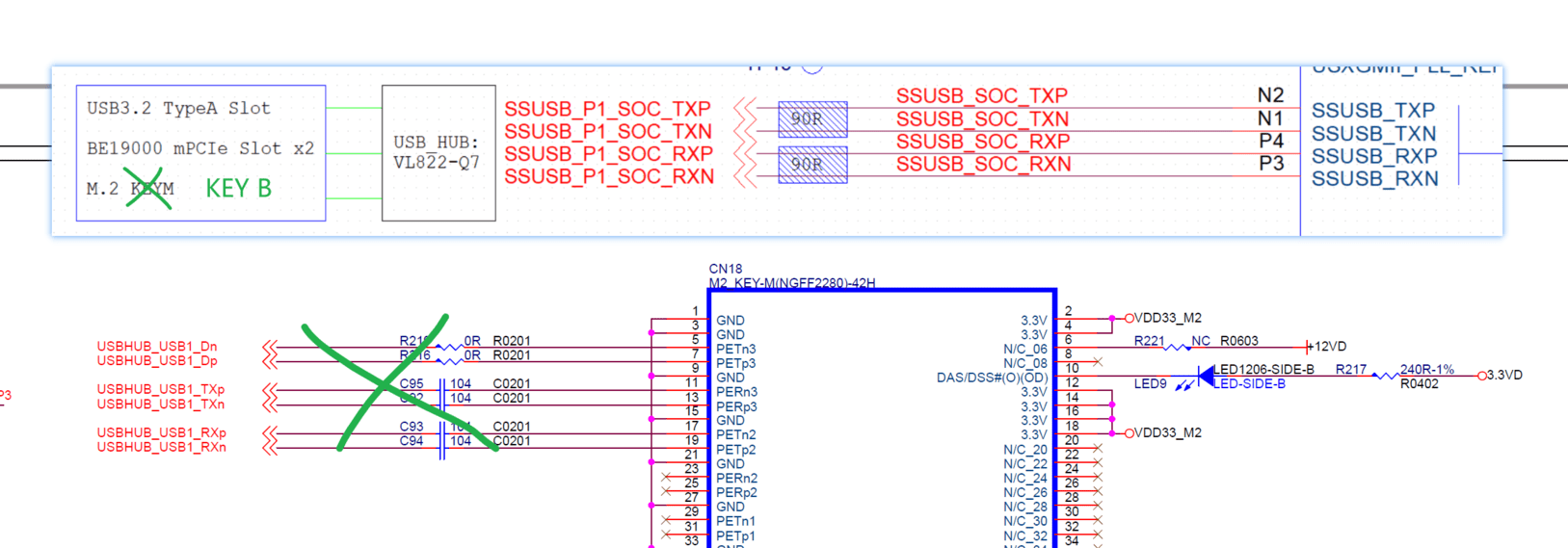
However, it is recommended that if you want to test 5G modems, you can plug it into the M.2 KEY-M through an adapter board. We have reserved the fourth USB3.0 port of the USB-HUB to KEY-M(non-standard)
It can be powered with PD, using CH224K.
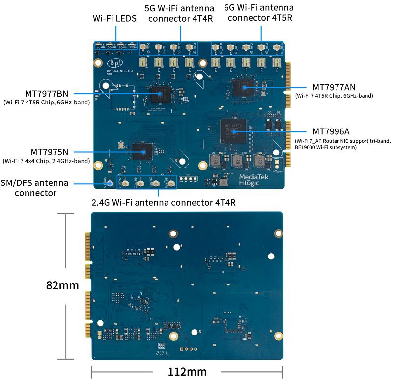
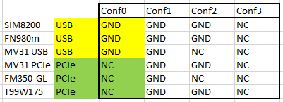
Banana Pi BPI-R4 wifi7 module use MediaTek MT7996+MT7995+MT7977A+MT7977B chip design.
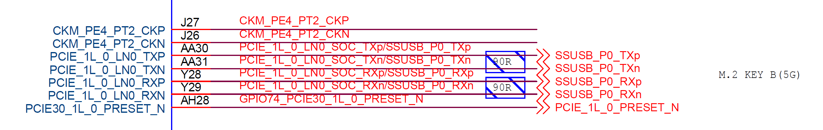
According to block diagram of BPI-R4, M.2 key B connector for 5G has USB3 and PCIe . Is that correct?
If yes, than cheaper 5G modules could be used, like FM350-G or T99W175 that uses PCIe intead of USB.
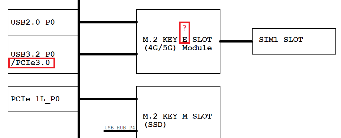
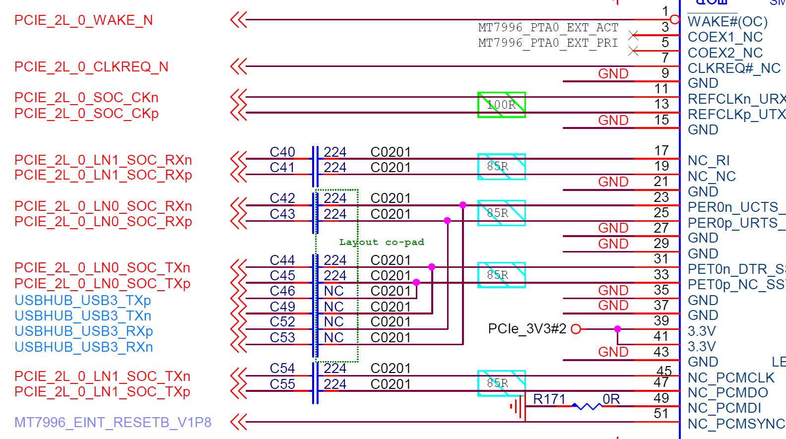
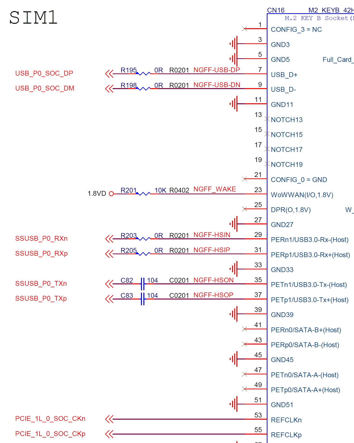
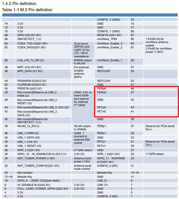
USB3.0 on M.2 KEY-B is combo with PCIE_1L_0
Can you publish full shematic? Have you added coupling capacitors on the tx lines of pcie on all slots (known problem on other boards)?
Thanks for schematics.
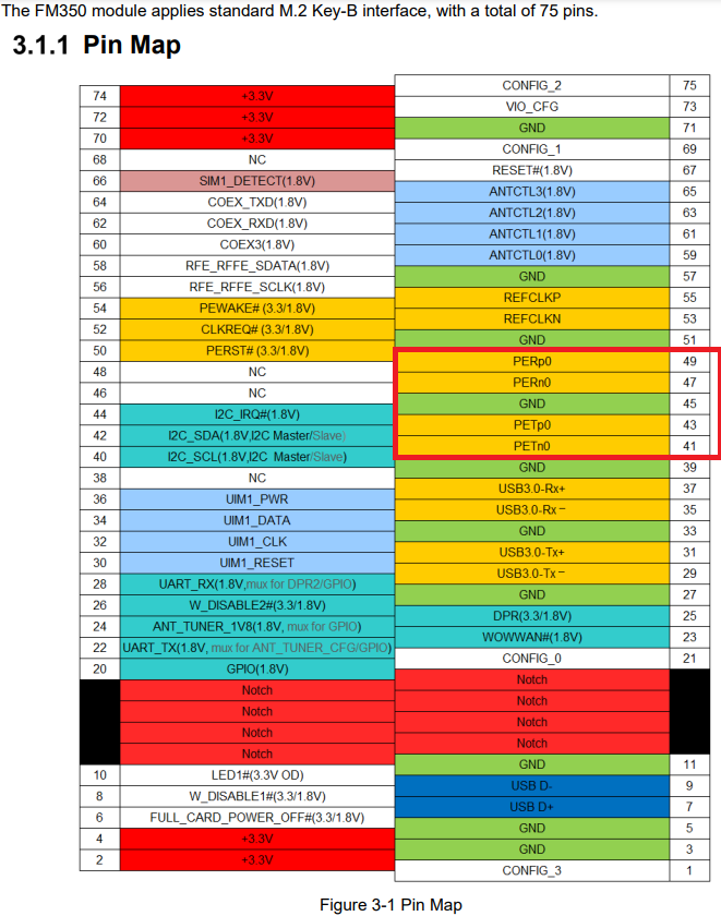
It seems that FM350 and T99 uses PCIe lane 0 (pins 41 - 49).
Is it possible to add at least resistors to switch from lane 1 to lane 0 in nice way?
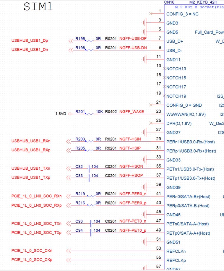
 http://219.143.15.28:3088/esurfing/tim/pim/20210430172231_100759345.pdf
 http://219.143.15.28:3088/esurfing/tim/pim/20201105162420_100320126.pdf
If BOM could stand one more IC - PCIe MUX could be used, i. e. PI3PCIE3212 https://www.diodes.com/assets/Datasheets/PI3PCIE3212.pdf
SEL pin could be driven by CONFIG_0 signal from M.2 connector :
I am not quite certain how others feel about it but I feel quite disappointed seing a hardware upgrade of a device which hasn’t already received official software support. Namely the BPI-R3.
I do understand that there is a proprietary OpwnWRT but that is not really a solution given the lack of software updates and, quite frankly, very old OpenWRT version the BPR-R3 is shipped with.
The Arm a57 also offers a serious performance increase making the R4 the more future proof choice. Future proofness and open source were my main motivators opting for the BPI-R3.
Really disappointing 
Edit: There is already a great article out there which partially compared the R3 to the R4
Whilst the R3 is not obsolete per se since it still offers one of the most compelling and performant hardware specs compared to off the shelf products, the R4 looks hell of a lot more compelling given the plethora of storage options, doubled RAM, better overall design with the antenna ports moved to the bottom of the PCB.
In particular moving the antenna ports show how much brain power was invested. The LEDs are also better placed enabling properly light carriers instead of the flimsy 1mm at most spacing on the R3. Not to speak of the (presumably) much improved BootStrap switches which, quite frankly, still give me some headache.
1 Like
It’s not the time yet, there’s still a lot to change,it may be released later.
Yes, All have added coupling capacitors. 
Thank you for your suggestions and datasheet!
Because the PCB layout now has not much space to add additional IC.Maybe we change like this:
DTS changed SSUSB_P0 to PCIE_1L_0, then connected to pins 41-49 of KEYB, and routed the USB3.0 on KEYM to KEYB pins 29-37.
make the voltage of KEYB to 3.6V, so that the 5G module can run more stably.
Simple and efficient 
I see that there are two M.2 and two miniPCIe connectors. M.2 have one PCIe lane each, miniPCIe two PCIe lanes each. Is that correct?
Are there any limits for PCIe usage or all four PCIe controllers are available?
then the bpi-page is wrong as it states only usb there:
- 1x M.2 KEY-B slot with USB3.2 interface for 5G
- 1x M.2 KEY-M slot with PCIe3.0 1lane interface for NVME SSD
how much pcie-controllers has mt7988? 2x1Lane and 2x2lane?
are really 4 pcie3 lanes needed for wifi-nic?